
- All
- Product Name
- Product Keyword
- Product Model
- Product Summary
- Product Description
- Multi Field Search

 |


| Quantity: | |
|---|---|
Product Feature
·PS material
·Various patterns, sizes and shapes can be customized
·Stable anti-static
·Embossed surface
·Easy to Grasp
·For cleanroom
Product Specification
型号 Model | 材质 Material | 英寸(in) Size | 直径(mm) Diameter | 表面电阻值 (Ω/Sq) Surface Resistance | 薄膜厚度(μm) Thickness | 花纹样式 Surface | 备注 Remark |
JH5063PS | 聚苯乙烯 PS | 4/5/6/6.5/7/8/10/ 11/12/14/15/16 | 100/125/150(152,155)/165/180(178) /200(203)/254/275/300(299,305)/360 /380(390)/400/定制 Customized | 100K-1G | 100/定制 Customized | 方格/单面点状/平面/定制 Embossed with squares or dots/smooth/Customized | -- |
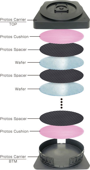
Advantages of HAOUGER Embossed Semiconductor Wafer separators for Back End :
·Embossed Semiconductor Wafer separators for Back End are widely used in the separate packaging of multi/monocrystalline silicon wafers such as solar cells, wafers, and solar silicon wafers.
·HAOUGER Embossed Semiconductor Wafer separators for Back End can be customized with shapes, diameters, surface patterns.
·HAOUGER has plenty of experience in making and using wafer separators, we provide products with high quality, low price and short lead time.
Product Feature
·PS material
·Various patterns, sizes and shapes can be customized
·Stable anti-static
·Embossed surface
·Easy to Grasp
·For cleanroom
Product Specification
型号 Model | 材质 Material | 英寸(in) Size | 直径(mm) Diameter | 表面电阻值 (Ω/Sq) Surface Resistance | 薄膜厚度(μm) Thickness | 花纹样式 Surface | 备注 Remark |
JH5063PS | 聚苯乙烯 PS | 4/5/6/6.5/7/8/10/ 11/12/14/15/16 | 100/125/150(152,155)/165/180(178) /200(203)/254/275/300(299,305)/360 /380(390)/400/定制 Customized | 100K-1G | 100/定制 Customized | 方格/单面点状/平面/定制 Embossed with squares or dots/smooth/Customized | -- |
Advantages of HAOUGER Embossed Semiconductor Wafer separators for Back End :
·Embossed Semiconductor Wafer separators for Back End are widely used in the separate packaging of multi/monocrystalline silicon wafers such as solar cells, wafers, and solar silicon wafers.
·HAOUGER Embossed Semiconductor Wafer separators for Back End can be customized with shapes, diameters, surface patterns.
·HAOUGER has plenty of experience in making and using wafer separators, we provide products with high quality, low price and short lead time.


